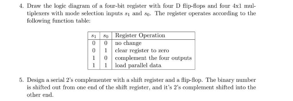
Serial 2 S Complementer Shift Register
пятница 01 марта admin 41
Just to be fair, this is a previous exam question and was an assignment question. I've already handed in the assignment and now I'm trying to see why I got it wrong -- to study for my final.
Design a serial 2s complementer with a shift register and a. Design a serial 2s complementer with a shift register and a flip-flop. Request for Solution File. Design a serial 2's complementer with a shift register and a flip flop. The binary number is shifted out from one side and it's 2's complementer shifted in to the other side of the shift register.
I fully understand how to find the 2's complement of a binary number, however, implementing a circuit to find the complement is driving me crazy. I'm given a shift register (that stores my binary number) and a flip flop (using D for simplicity). The process I follow for building sequential circuits is this: • I look at the question and derive a state diagram. • From the state diagram, I draw a state table and find the input of my flip flops • I use maps and stuff to finally build the circuit. I'm trying to visualize how to actually draw the state diagram for this complementer.
I know it depends on the previous value and stuff, but if someone could take the time to explain in plain english how he/she would go about building the state diagram, I would be vey grateful. That link you gave says it all: Hint: - 2’s complement of a number can be obtained by keeping the least significant bits as such until the first 1, and then complementing all bits 'example 001010 → 110110' that is to say 001010 -> flip bits -> 110101 -> add 1 -> 110110 msb lsb msb lsb msb lsb msb lsb input 001010 output 110110. You know the 2's complement of each of the binary values 0000, 0001, 0010, 0011. There are at least 2 ways to get the 2's complement of a number in a SIPO shift register: • direct combinatorial logic. Operation research by pkgupta and dshira free. Take the 4 bits of the value, (simultaneously) invert all the bits and (simultaneously) add one.
(I think a bunch of half-adder circuits are adequate here -- you can copy those out of your textbook, right?) There is no flip-flop or other internal state with this approach. • Serial incrementer. Starting with the least-significant bit, shift one bit at a time into a serial incrementer (a single half-adder and a single D flip flop).
The serial incrementer generates (one bit at a time), from the current bit from the shift register and a Carry_in bit, the Carry_out bit and the Sum bit. Every clock cycle, the old Carry_out bit is latched into your D flip flop and becomes the new Carry_in bit, and the next bit comes out of the shift register. Then the half-adder combinational logic combines them to produce another Carry_out bit and Sum bit. Libros cristianos. (The flip-flop also needs some way to reset the carry bit it holds to '1' when starting over with the least-significant bit of a new number).
When adding 2 bits, the Carry_out is 1 only when both bits are 1; otherwise the Carry_out is zero.

Hey guys, so the question reads: It is known that the 2's complement of a binary number can be formed by leaving all significant 0's and the first 1 unchanged and complementing all other higher bits. Design a serial 2's complementer using this procedure. The circuit needs a shift register to store the binary number and an SR flip flop to be set when the first least significant 1 occurs. An XOR gate can be used to transfer the unchanged bits (x[xor]0=x) or complement the bits (x[xor]1=x'). So i understand all the components in the circuit, like the register, the xor gates, and the SR, but i have no idea about how to mesh them together to form this circuit Any help would be mucho appreciatedo!